By: George Che, PhD Candidate, Exploration Systems Design, School of Earth & Space Exploration, ASU
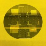
What did the universe look like immediately after the Big Bang? What are the mechanisms that drive star formation? How do galaxies evolve over time? Answering these questions requires extremely precise observations of light from the sky outside the range of human eyesight. Central to both scientific and commercial applications, the dominant photodetector technology for light visible to the human eye is the charge-coupled device (CCD), which is found in both the Hubble Space Telescope and smartphone camera in your pocket. While visible light astronomy has yielded many profound insights, observations across the electromagnetic spectrum are necessary for a more complete understanding of our universe. Arrays of KIDs on a thin 4-inch wafer fabricated in the CSSER NanoFab In particular, the microwave portion of the spectrum contains a plethora of information about the formation of both individual objects and overall structure of the universe. CCDs cannot detect microwaves, so we need a fundamentally different photodetector to do this type of astronomy. This photodetector is the kinetic inductance detector (KID), which is an ultrasensitive detector realized as a superconducting integrated circuit. Because KIDs are superconducting detectors, they need to be cooled to cryogenic temperatures for operation. For my research, I develop KID-based astronomical instruments that push the boundaries of sensitivity, resolution, and bandwidth. Currently, the nascent KID technology finds its application predominantly in science, but has the potential to enable significant progress in passive imaging for defense and security applications.
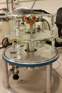
A significant portion of my work is dedicated to fabricating prototypes of novel KID designs and related devices. Multi-stage cryogenic system to cool KIDs to requisite temperature The metal deposition, photolithography, etching, and metrology tools in the CSSER NanoFab provide me the capability to fabricate my devices in-house at ASU, greatly reducing both cost and lead time. Starting from a bare wafer, I deposit thin superconducting films (e.g. aluminum and niobium) using electron beam evaporation and sputtering tools. I then use the photolithography and etching tools to pattern the film, defining the integrated circuits. Metrology is used for physical and electrical characterization to validate each step of the fabrication process. Utilizing many pieces of CSSER’s microfabrication equipment and working closely with its highly knowledgeable staff has enabled me to make significant contributions to multiple large-scale astronomical instrumentation projects funded by the National Science Foundation and NASA.
Arriving at ASU in 2012, I am an Exploration Systems Design PhD candidate in the School of Earth & Space Exploration. I will defend my dissertation this fall and receive my MSE in Electrical Engineering this summer. After graduation, I would like to apply my skills in electromagnetics, microwave circuits, and microfabrication to an engineering career with a government agency or in private industry