By Ray Tsui, Ph.D.
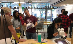
ASU, Tempe campus, held its 2018 open house on Feb. 24th. This annual signature event, now renamed ASU Open Door, invites the general public to visit and learn about the wide-ranging work and capabilities of the university. NCI:SW participated in this well attended event by hosting the exciting activity called “Look Inside the Nano World.”
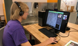
Silicon wafers, 300 mm-diameter, that were processed through a fab line were used to introduce visitors to unique aspects of nanotechnology. An optical microscope was available to view details on the wafers. Then, access to a remotely-located scanning electron microscope was engaged to allow visitors to control the imaging of various samples that ranged from an insect to nanowires at high magnification. Allowing viewers to learn more about micro- and nanoscale technology.
In all, there were over 700 visitors, of all ages, enjoying the exhibits and demonstrations. Making it a true K-to-Gray learning experience.