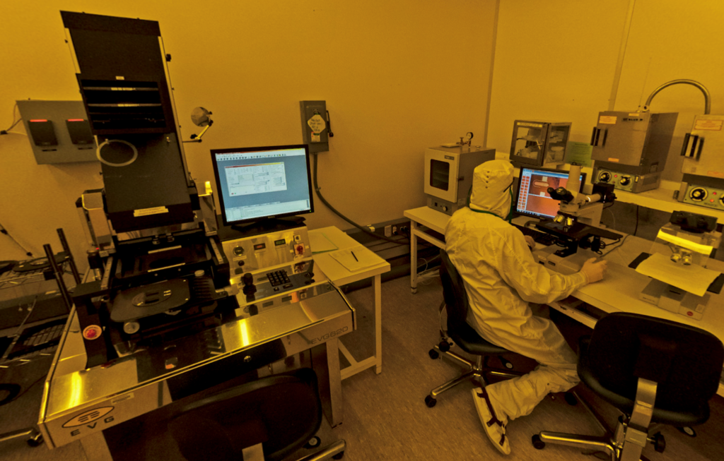
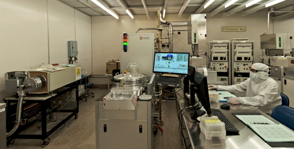
Whether you are a teacher or faculty member, introducing a group of students, or an industry member wanting to explore collaborative research possibilities, we welcome you to tour the NanoFab. Contact us to pre-arrange your visit. NanoFab is located at the Engineering Research Center on ASU’s Tempe campus. Contact Dr. Raymond Tsui..