Integrated Nanophotonics was the subject of the Oct. 17, 2019 NCI-SW webinar.
Consider, the combination of those two words, nano and photonics, with the goal of moving signals around with light, as we would do with electricity. The key technology device is called a PIC, Photonics Integrated Circuit. View the recording here.
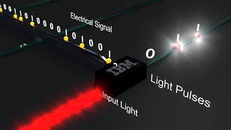
The use of telecommunications discrete photonics components has dramatically increased data transmission. View the figure below, that illustrates the concept of transduction of electrical signals into light pulses.
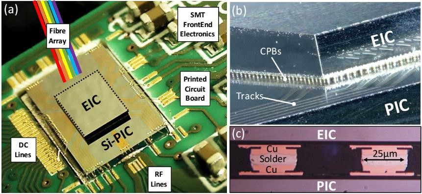
A primary take-away from this webinar was that the technology innovations of creating nano feature sizes with lithography allowed the fabrication of this photonic light sources and detectors onto silicon, leading to the integration of photonics with chip technology. This led to high volume manufacturing, which means the devices could become real products used in many applications. Below you can see how an electronic integrated circuit is integrated with a PIC.
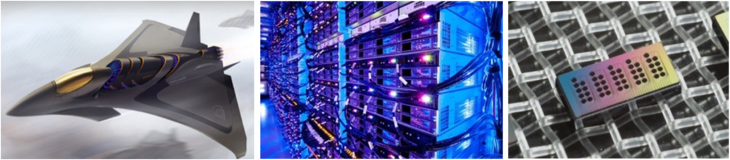
What does this mean for applications? Defense and computing: lighter, faster, more compact. Data centers and server farms are more efficient and use less energy; the world is more connected. Real time detection of bio markers through labs on a chip becomes more feasible.
Our expert presenter, Dr. Bob Geer, from SUNY Polytechnic addressed what this means for preparing students for the skilled technical workforce. Data acquisition and analysis, for example, is growing in importance and typically a technician would conduct:
- Multi-power data acquisition
- Collation/documentation (data port to plot & analysis)
- Document for engineer team report

Professor Geer showed what those typical new skills looked like, how they would fit, and said there are a lot of resources availble to help educators “Think NanoPhotonics!” This fall webinar provided great information for those in research and industry.