DIAMOND:
THE NEW ‘WONDER MATERIAL’ FOR EXTREME ENVIRONMENT ELECTRONICS
Most commercial electronics these days is manufactured from semiconductors such as silicon and gallium arsenide. While Si and GaAs were the original ‘wonder materials’ that allowed the enormous progress microelectronics epitomized by Moore’s law they have certain limitations that prevent them from being used in extreme environments. For example, while silicon-based electronics struggles to operate above 200° C, there are numerous applications from automotive electronics, to DC-DC power conversion, and space communications that would benefit from the ability to operate at temperatures of 300° C and above. The new ‘wonder materials’ being designed for extreme applications are often referred to as ultra-wide bang gap (UWBG), and amongst these diamond is looking very attractive. Part of the attraction for diamond is its extremely high thermal conductivity that is approximately 30 times higher than that of silicon. As a result, a diamond-based device can efficiently dissipate heat that would otherwise lead to catastrophic failure in a silicon device. An example of this is the radio frequency power amplifier used in cell phone towers for mobile device communication. At present these RF PAs have elaborate colling requirements that could be greatly simplified if an equivalent diamond device was available. The same is true for satellite-based communication and radar systems, but these also have to survive the hostile radiation environment of space. Again the natural properties of diamond make it intrinsically radiation tolerant and therefore ideally suited for space electronics.

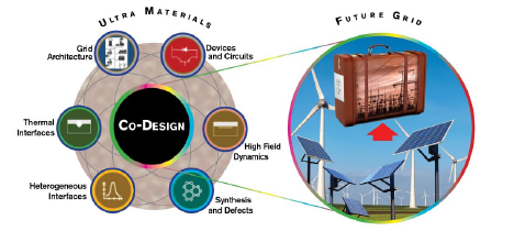
The ULTRA EFRC combines expertise from different disciplines to ‘co-design’ the electrical power grid of the future.
Efficient electrical energy conversion is another area that would benefit from the high power handling capabilities of UWBG materials. The ULTRA Center at ASU is a DOE Energy Frontier Research Center (EFRC) funded with a four year, $12.4M award. The ULTRA EFRC is directed by ASU Regents’ Professor Robert Nemanich, and has the goal of making power conversion more compact and efficient. Imagine a typical neighborhood electrical substation being replaced by a suitcase sized power converter.
Nemanich and his team are frequent users of the ASU NanoFab and Eyring Materials Center core facilities. He also works with Advent Diamond, an ASU ‘spin-off’ company that is developing diamond-based sensors for neutron and x-ray detection. A recent article in Physics Today explores these projects and other exciting new developents, as well as some of the challenges we need to overcome for high volume diamond electronics manufacturing to become a reality.