Panagiotis Theofanopoulos, PhD Student, Electrical, Energy, and Computer Engineering, Ira Fulton Schools of Engineering
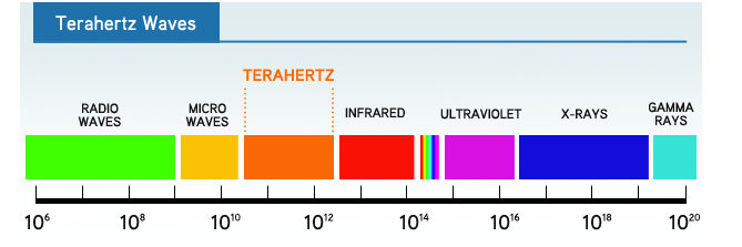
In the terahertz regime, wavelengths range from millimeters to submillimeters and the frequencies from 30 GHz up to 10 THz (see the frequency diagram below.) We will refer to them as mmW/THz waves.

Source: https://www.nanalyze.com
Specifically, all waves are identified by two inversely proportional metrics, wavelength and frequency: as frequency increases, wavelength decreases and vice versa. For instance, the microwaves that we use to heat our food have low frequencies but big wavelengths (a few cm); conversely, the infrared cameras that are embedded in the new smartphones have high frequencies and tiny wavelengths (nanometer scale). Millimeter and terahertz waves are in between with relatively high frequency and small but not tiny wavelengths (milli/micrometer scale). These characteristics allow for high-spatial-resolution imaging compared to microwaves due to smaller wavelengths, but lower losses than higher frequencies. In addition, mmW/THz waves are harmless for humans, unlike X-rays.
Until recently, this part of the electromagnetic spectrum was unexplored due to the lack of equipment (sources, sensors etc.). However, scientists revealed that the small wavelengths of mmW waves can lead to very interesting applications including radars that “see” through clothing (e.g. the airport scanners), sensors that image the underlying skin traits for biometric applications, and non-line-of-sight imaging. The latter is the main scope of our research, namely, we use mmW/THz waves to “see” through the reflections on the walls, ceiling, and other surrounding surfaces. Namely, THz waves scatter from these surfaces as visible light scatters from mirrors. Due to their longer than light wavelength, these “optically” rough surfaces appear polished under mmW/THz illumination. Hence, we can exploit them as mirrors to “see” objects that are not in our line of sight.

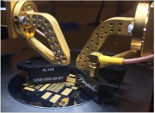
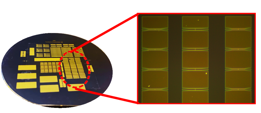
But, how can you “see” when you are blind? Our eyes cannot detect these frequencies as mentioned above; therefore, we need sensors/radars to “see” for us. These sensors are in the microscopic scale (smaller than the diameter of the human hair); hence, to develop them we need advanced fabrication techniques and cleanroom facilities like ASU-NanoFab. In our fabricated topologies, we embed graphene, which is a controllable 2D material, to create low-profile switchable sensors. These sensors form antenna arrays that are exploited to acquire high-quality images using mmW/THz waves. Using the ASU-NanoFab facilities, we have developed and tested novel nano-fabrication processes including wet/dry etching, metal sputtering, and sacrificial layers, for devising graphene switched configurations. These processes enable the development of large-scale graphene-controlled antenna arrays for the first time.

We are still are exploiting the state-of-the-art facilities of ASU-Nanofab to fabricate our prototypes, so we can continue exploring the interesting applications of mmW/THz waves. Further information about our research is available on our website.

Panagiotisis a PhD student at Electrical Engineering, Ira A. Fulton Schools of Engineering at Arizona State University. He received his Diploma (5-year studies) and Master degree in Electrical and Computer Engineering from Democritus University of Thrace (DUTH), Xanthi, Greece, in 2013 and 2015 respectively. His research interests are computational electromagnetics, antennas, microwave, and THz devices.